


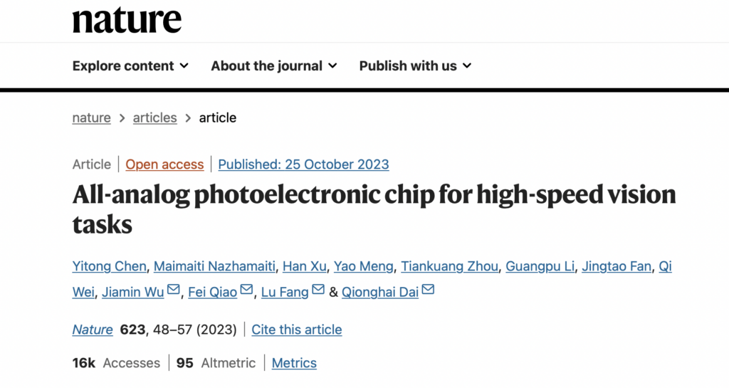
Recently, several Chinese academicians at Tsinghua University, collaborated to achieve a key breakthrough in the field of chips. They developed the ACCEL photonic computing chip, which, in several complex intelligent visual tasks, achieved the same accuracy as existing high-performance chips, while demonstrating an international first with a computing power increase of over three thousand times and an energy efficiency improvement of over four million times. The related achievements were published in the journal Nature.
If we were to compare the time it takes for information flow calculations in the chip to the time taken by a mode of transportation, the appearance of this chip is equivalent to shortening an 8-hour journey on a high-speed railway to 8 seconds.
In this small chip, Tsinghua University’s research team creatively proposed a computing framework for the deep integration of optoelectronics. Starting from the most fundamental physical principles, it combines optical computing based on the spatial propagation of electromagnetic waves with pure analog electronic computing based on Kirchhoff’s law.
The design breaks the physical bottleneck of data conversion speed, precision and power consumption constraints of the traditional chip architecture. Moreover, it successfully tackles three international challenges: large-scale integration of computational units, high-efficiency nonlinear, and high-speed optical-electronic interfaces on a single chip, thus resolving optoelectronic interface issues at the international level.
Under the actual performance, the system-level computing power of the photoelectric fusion chip is thousands of times higher than that of the existing high-performance chip architecture.
In the intelligent vision tasks and traffic scenarios demonstrated by the R&D team, the photovoltaic fusion chip’s system-level energy efficiency (the number of operations that can be performed per unit of energy) was measured to be 74.8 Peta-OPS/W, which is more than four million times higher than that of existing high-performance chips. Figuratively speaking, the power that was originally used to power an existing chip for one hour can be used to power it for more than five hundred years.

A key factor limiting the limit of chip integration at present is the heat dissipation problem brought about by excessive high density. The optoelectronic fusion chip running at ultra-low power consumption will help to significantly improve the chip heat problem, bringing a full range of breakthroughs to the future design of the chip.
Further, the minimum line width of the optical part of the chip is only 100 nm, while the circuit part is only 180 nm CMOS process, which has achieved many orders of magnitude of performance improvement over the 7nm high-performance chips.
At the same time, the materials used are simple and easy to obtain, and the cost is only one tenth of the latter. It can be foreseen that as China’s chip processing technology continues to improve, more new materials will join the future.
The development of this new computing architecture opens up a new path for future technologies to enter daily life and inspires the integration of other high-efficiency technologies like quantum computing and in-memory computing with current electronic information systems.
One of the corresponding authors, Academician Dai Qionghai of Tsinghua University, emphasizes the importance of not only developing a new computing architecture for the AI era but also implementing it in real-life applications to address major national needs.
(Source: Institute of Automation, Chinese Academy of Sciences)